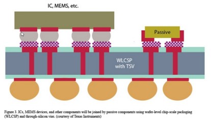
Wafer Level Package (WLP) is generally defined as performing most or all of the packaging and testing directly on the wafer, and then singulation to make a single component. And RDL, Bumping Copper pillar, TSV and other technologies are the key technologies of WLP. The focus of this issue is TSV. Through-Silicon-Via (TSV, Through-Silicon-Via) is the latest technology to achieve interconnection between chips by making vertical conduction between chips and between wafers and wafers. Different from the previous IC packaging bonding and the use of bump superimposition technology, TSV can maximize the stacking density of the chip in the three-dimensional direction, the smallest size, and greatly improve the chip speed and low power consumption performance. TSV is a key technology for 2.5D and 3D packaging.

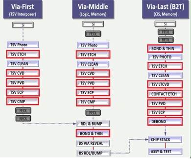
Based on the existing key packaging equipment, Yoshinaga Corporation aims at the commanding heights of the industry and vigorously expands the 2.5D/3D WLP packaging business of TSV technology interconnection. Cooperating with Japanese manufacturers such as EBARA, ULVAC, OKAMOTO, TOK, etc., launched Coating, Etching, CVD, PVD, Plating, CMP, Temporary Bonding and De-bonding, Wafer Thinning and other TSV special process equipment solutions. At present, our company can provide processing equipment in the red frame, and Yoshinaga is the only company that can provide the entire line of TSV processing solutions. (Editor: Jeff.Lee)

|


